ASUS ROG GA503RS-LN006W RAM upgrade specifications




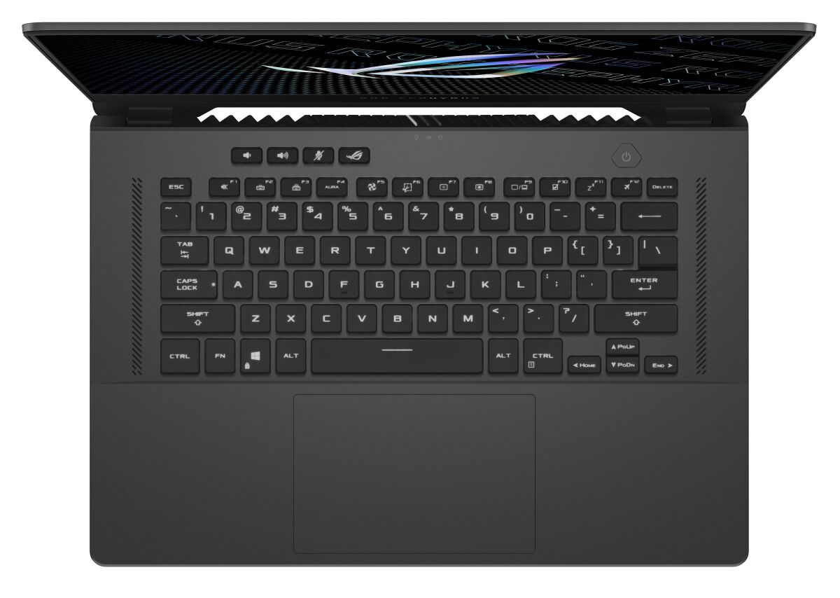
The ASUS ROG Zephyrus G15 GA503RS-LN006W features DDR5-SDRAM memory upgrade capability with one SO-DIMM slot available for expansion. The laptop contains on-board memory paired with one upgradeable SO-DIMM slot, supporting a maximum RAM capacity of 48 GB. Compatible memory modules operate at 4800 MHz frequency. Users can upgrade the single SO-DIMM slot to enhance overall memory specifications and system performance for this gaming laptop model.
Memory Upgrade Specifications
| Specification | Value |
|---|---|
| Memory slots | 1x SO-DIMM |
| Form factor | On-board + SO-DIMM |
| Memory type | DDR5-SDRAM |
| Frequency | 4800 MHz |
| Maximum RAM | 48 GB |
| Voltage | 1.1V |
| Number of pins | 262-pin |
| Interface | PC5 |
| PC Speed Rating | PC5-4800 (PC5-38400) |
| Bandwidth | 38.4 GB/s |
| Laptop Release date | 10 January 2022 |
Additional Notes
- The presence of a single SO-DIMM slot combined with on-board memory indicates that only 1 channel remains accessible for physical replacement or expansion.
- The 48 GB maximum capacity implies an asymmetrical memory configuration where a 32 GB module is paired with the fixed 16 GB on-board chips.
- Upgrading the **ASUS ROG GA503RS-LN006W** with a module that exceeds the native 4800 MHz frequency will result in the system downclocking the new hardware to match the fixed speed of the integrated memory.
- Dual-channel performance is contingent on matching the capacity of the removable module to the soldered memory, otherwise the system will operate in flex mode where only a portion of the total RAM utilizes full bandwidth.
- System stability depends on using non-ECC unbuffered modules because the motherboard architecture does not support error-correcting code correction despite the DDR5 standard including on-die ECC.
- Internal access for maintenance requires the removal of the bottom chassis panel, which exposes the single expansion slot for immediate density increases without disturbing the integrated primary memory bank.
- Latency timings are governed by the slower of the two memory banks, meaning high-performance aftermarket modules will be restricted by the factory-set CL values of the on-board silicon.