ASUS TUF Gaming FX507VI-LP097W-GAMING RAM upgrade specifications




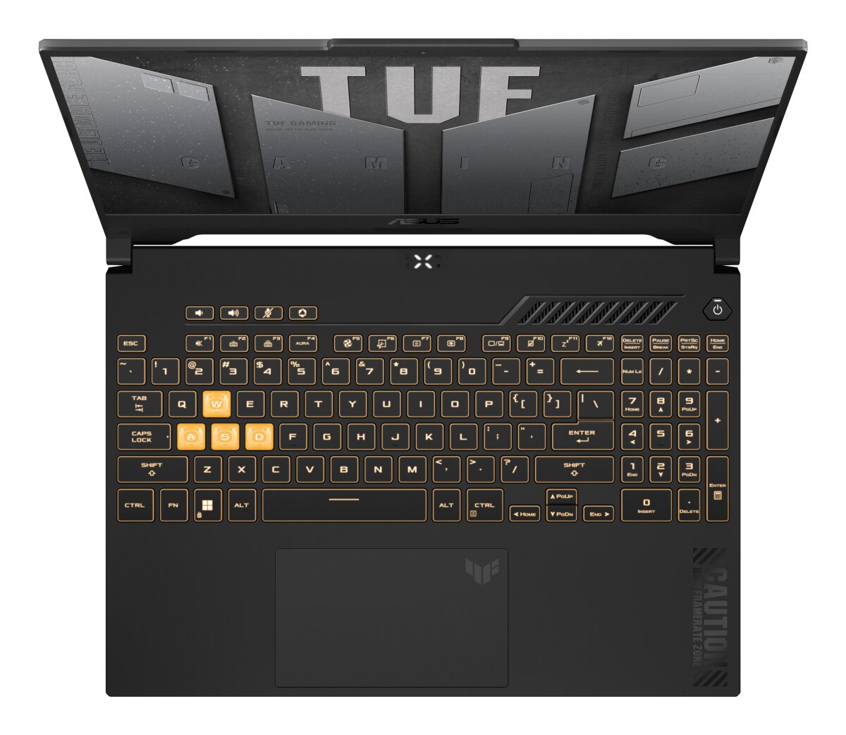
The ASUS TUF Gaming F15 series model FX507VI-LP097W-GAMING features DDR5-SDRAM memory with two SO-DIMM upgrade slots. The laptop supports maximum RAM capacity of 32 GB total. Compatible memory modules operate at 4800 MHz frequency and utilize SO-DIMM form factor. Specifications indicate the device accommodates DDR5 memory upgrades for enhanced performance and multitasking capabilities.
Memory Upgrade Specifications
| Specification | Value |
|---|---|
| Memory slots | 2x SO-DIMM |
| Form factor | SO-DIMM |
| Memory type | DDR5-SDRAM |
| Frequency | 4800 MHz |
| Maximum RAM | 32 GB |
| Voltage | 1.1V |
| Number of pins | 262-pin |
| Interface | PC5 |
| PC Speed Rating | PC5-4800 (PC5-38400) |
| Bandwidth | 38.4 GB/s |
Additional Notes
- The 32 GB ceiling reflects Intel platform limitations rather than physical slot restrictions, potentially affecting users with multi-virtual machine workflows or large dataset processing requirements.
- DDR5 voltage regulation moves from motherboard to module level, requiring PMIC-equipped SO-DIMMs and eliminating compatibility with older DDR4 inventory.
- JEDEC baseline 4800 MHz specification suggests unlocked multiplier access may enable higher frequency operation through XMP 3.0 profiles, though thermal headroom in the ASUS TUF Gaming FX507VI-LP097W-GAMING chassis becomes the limiting factor.
- Dual-channel population mandates matched module pairs for symmetric bandwidth allocation, as mismatched capacities force asymmetric mode with reduced effective throughput on the larger module.
- On-die ECC functionality in DDR5 architecture operates transparently without OS visibility, correcting single-bit errors at the DRAM level before data reaches the memory controller.
- SO-DIMM 262-pin keying prevents insertion errors, but mixing modules with different die densities can trigger training failures during POST despite matching speed ratings.
- Soldered CPU memory controller means RAM stability directly impacts system longevity, as controller degradation from voltage overstress cannot be remedied through motherboard replacement.
- Reduced 1.1V operating voltage compared to DDR4's 1.2V lowers thermal output per module, though doubled prefetch buffer from 8n to 16n increases latency sensitivity in single-threaded applications.
- JEDEC-standard modules lack RGB controller overhead, freeing I2C bus bandwidth and reducing potential firmware conflicts with iCUE or Armoury Crate lighting ecosystems.
- Bank group architecture expansion to 4 groups in DDR5 improves parallelism for multi-threaded workloads but complicates memory training algorithms, extending cold boot times by 2 to 4 seconds compared to DDR4 systems.