MSI Gaming GF65 9SD-074 Thin RAM upgrade specifications



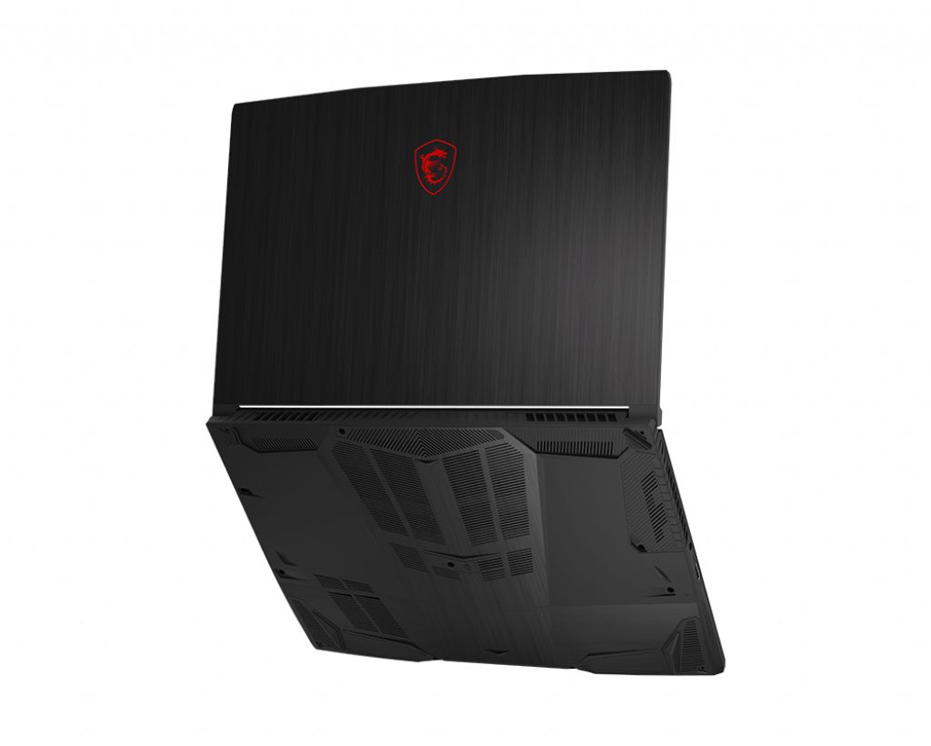
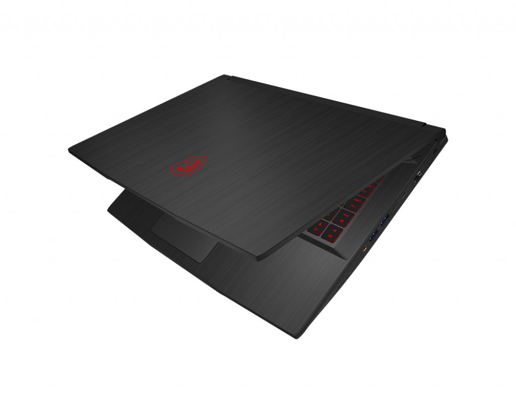
The MSI GF65 9SD-074 Thin Gaming series laptop features DDR4-SDRAM memory upgrade specifications with 2x SO-DIMM slots supporting maximum capacity of 64 GB RAM. Compatible memory operates at 2666 MHz frequency. The upgrade slots accommodate SO-DIMM form factor modules, enabling users to expand memory capacity for enhanced multitasking performance. Specifications indicate compatibility with standard DDR4 memory modules meeting the GF65 9SD-074 Thin requirements.
Memory Upgrade Specifications
| Specification | Value |
|---|---|
| Memory slots | 2x SO-DIMM |
| Form factor | SO-DIMM |
| Memory type | DDR4-SDRAM |
| Frequency | 2666 MHz |
| Maximum RAM | 64 GB |
| Voltage | 1.2V |
| Number of pins | 260-pin |
| Interface | PC4 |
| PC Speed Rating | PC4-2666 (PC4-21328) |
| Bandwidth | 21.3 GB/s |
| Laptop Release date | 18 December 2019 |
Additional Notes
- The MSI GF65 9SD-074 Thin accepts only DDR4 SO-DIMM modules, excluding desktop-sized DIMMs and older DDR3 variants regardless of physical adapters.
- The 2666 MHz frequency specification represents the maximum officially supported speed, with higher frequency modules automatically downclocking to this threshold.
- The 64 GB ceiling requires 2 modules of 32 GB each in dual-channel configuration, as single-module capacity cannot exceed this architectural limit.
- Mixing different capacity modules between slots remains functional but forces operation in asymmetric or flex mode, reducing memory bandwidth compared to matched pairs.
- The chipset enforces non-ECC unbuffered memory exclusively, making registered or error-correcting modules incompatible despite matching physical dimensions.
- Voltage requirements default to 1.2V standard for DDR4, with low-voltage 1.35V SO-DIMMs causing potential stability issues or boot failures.
- The dual SO-DIMM architecture necessitates bottom panel removal for access, with specific screw patterns potentially voiding warranty seals depending on regional service policies.
- Thermal constraints in this chassis design prioritize single-sided memory modules over double-sided variants to maintain airflow clearance near heat-generating components.
- JEDEC standard timing profiles receive priority during POST, with XMP/AMP overclocking profiles disabled in most mobile BIOS implementations.
- The 9th generation Intel platform underlying this model lacks native support for frequencies exceeding 2933 MHz, rendering faster modules economically inefficient.